BIPOLAR JUNCTION TRANSISTOR
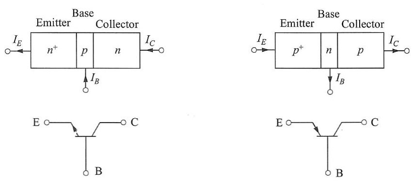
The transistor is a three-layer semiconductor device consisting of either two n- and one p-type layers of material or two p- and one n-type layers of material called an npn transistor and a pnp transistor respectively.
Bipolar junction transistors are made of a semiconductor material (usually silicon) and consist of three doped semiconductor regions: the emitter, the base, and the collector.
Emitter: The emitter is heavily doped with either electrons (for an NPN transistor) or holes (for a PNP transistor). It emits majority charge carriers (electrons or holes) into the base region.
Base: The base is lightly doped and physically located between the emitter and the collector. Its thickness is crucial for transistor operation. It controls the flow of charge carriers from the emitter to the collector.
Collector: The collector is also heavily doped, but with charge carriers opposite to those of the emitter. It collects the charge carriers emitted by the emitter.
Configuration Modes of a Transistor
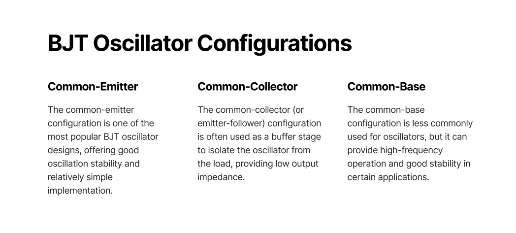
Bipolar Junction Transistors (BJTs) can be configured in three main configurations: Common Emitter (CE), Common Base (CB), and Common Collector (CC). Each configuration offers different advantages and is used in various circuit applications. Here’s a brief overview of each:
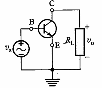
Common Emitter (CE): In the CE configuration, the emitter terminal is common between the input and output circuits. The input signal is applied to the base terminal, and the output is taken from the collector terminal. This configuration provides voltage amplification and current gain. It is the most commonly used BJT configuration for general-purpose amplifiers. The CE configuration provides both voltage and current gain, making it suitable for applications requiring high input impedance and moderate output impedance.
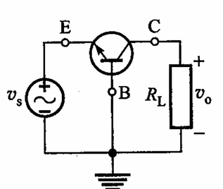
Common Base (CB): In the CB configuration, the base terminal is common between the input and output circuits. The input signal is applied to the emitter terminal, and the output is taken from the collector terminal. This configuration offers high-frequency response and current gain but does not provide voltage gain. CB configuration is often used in applications where high-frequency amplification is required, such as radio frequency (RF) amplifiers and oscillators.
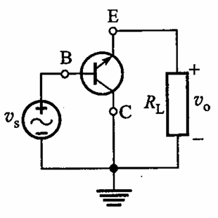
Common Collector (CC) (also known as the Emitter Follower): In the CC configuration, the collector terminal is common between the input and output circuits. The input signal is applied to the base terminal, and the output is taken from the emitter terminal. CC configuration provides high input impedance, low output impedance, and voltage gain slightly less than unity (less than 1). It is commonly used as a buffer amplifier to isolate the load from the preceding stages and provide impedance matching between circuits.
These configurations can be further modified and combined in various ways to achieve specific circuit requirements. The choice of configuration depends on factors such as input/output impedance requirements, gain, frequency response, and linearity needed for the particular application.

APPLICAITON OF BJT:
