Junction Field Effect Transistor (JFET)
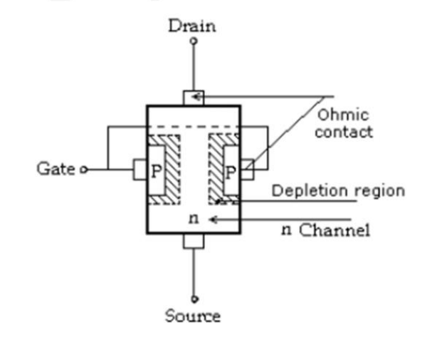
Junction Field Effect Transistor (JFET) The basic construction of n-channel FET is as shown in figure. The major part of JEET is the channel between embedded P types of material. The top of the n-channel is connected to an ohmic contact called as ‘Drain’ (D) & lower end of Channel is called as ‘Source’ (S). The two p types of materials are connected together & to the ‘Gate’ terminal (G). Here’s a basic overview of the construction of a JFET:
Semiconductor Material: The most commonly used semiconductor materials for JFET construction are silicon (Si) and gallium arsenide (GaAs). These materials provide the required electrical properties for JFET operation.
N-Type or P-Type Material: Depending on the type of JFET (N-channel or P-channel), the semiconductor material is doped to create either an excess of free electrons (N-type) or holes (P-type) in the material.
Channel Region: In the case of an N-channel JFET, the semiconductor material is typically N-type, and a narrow region of P-type material is created within it. This narrow P-type region forms the channel through which current flows when a voltage is applied.
Gate Region: On either side of the channel, there are heavily doped regions called the source and the drain. These regions are typically created by diffusing or implanting dopant atoms into the semiconductor material. The region between the source and the drain is called the gate region.
Insulating Layer (Optional): Some JFETs may have an insulating layer between the gate and the channel region to prevent direct contact between them. This insulating layer can be made of materials like silicon dioxide (SiO2).
Metal Contacts: Metal contacts are placed on the source, drain, and gate regions to allow for external connections. These contacts provide the terminals through which electrical signals are applied to or extracted from the JFET.

Characteristics:
As shown in the figure the gate is directly connected to source to achieve VGS = 0V, this is similar to no bias condition. The instant the voltage VDD (=VDS) is applied, the electrons will be drawn to the drain terminal, causing ID & IS to flow (i.e. ID = IS). Under this condition the flow of charge is limited solely by resistance of the n channel between drain & source. It is important to note that the depletion region is wider at the top of both p type of material.
As voltage VDS is increased from 0 to few volts, the current will increase as determined by ohm’s law. If still VDS is increased & approaches a level referred as VP, the depletion region will widen, causing a noticeable reduction in channel width. The reduced path of conduction causes the resistance to increase. The more the horizontal curve, the higher resistance. If VDS is increase to a level where it appears that the two-depletion region would touch each other, the condition referred as ‘pinch–off’ will result. The level of VDS that establish this condition is called as ‘pinch off voltage’ (VP). At VP, ID should be zero, but practically a small channel still exists & very high density current still flows through the channel. As VDS is increased beyond VP, the saturation current will flow through the channel (i.e IDSS).
(IDSS – Drain to source current with short cut connection from source to Gate.)
If a –ve bias is applied between gate and source, the effect of the applied –ve bias VGS is to establish depletion region similar to those obtained with VGS = 0V but at lower level of VDS. As VGS will become more & more –ve biased, the depletion layer pinch off occurs at the less & less value of VDS. Eventually, when VGS = – VP, will be sufficiently –ve to establish a saturation level, i.e. essentially 0 mA & for all practical purpose the device has been ‘turned OFF’. The region to the right of the pinch–off locus is typically employed in linear amplifiers (Amplifier with minimum distortion at applied signal) is commonly referred as the constant current, saturation or linear amplification region.


