Metal Oxide Semiconductor Field Effect Transistor (MOSFET)
The metal–oxide semiconductor field-effect transistor (MOSFET) is a transistor used for amplifying or switching electronic signals.
MOSFETs can be broken down into two types enhancement type and depletion type which are further classified into two types n-channel and p-channel MOSFET.
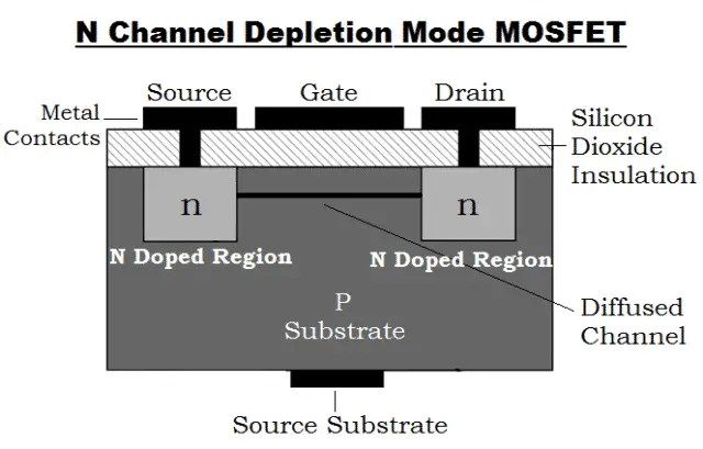
Depletion type MOSFET: In this type of MOSFET, channel is present from the beginning which means conduction of current is there. Negative voltage is applied to reduce the flow of current and this reduces the width of the channel. Not used commonly in devices.
Construction:
n-channel: A slab of p-type material is formed from a silicon base and is referred to as the substrate. It is the foundation upon which the device will be constructed. In some cases, the substrate is internally connected to the source terminal. However, many discrete devices provide an additional terminal labeled SS, resulting in a four-terminal device. The source and drain terminals are connected through metallic contacts to n-doped regions linked by an n-channel as shown in the figure. The gate is also connected to a metal contact surface but remains insulated from the n-channel by a very thin silicon dioxide (SiO2) layer. SiO2 is a particular type of insulator referred to as a dielectric that sets up opposing (as revealed by the prefix di-) electric fields within the dielectric when exposed to an externally ap plied field.
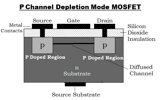
p-channel: The construction of a p-channel depletion-type MOSFET is exactly the reverse of that of n-channel. That is, there is now an n-type substrate and a p-type channel.
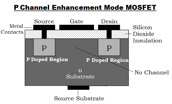
Enhancement type MOSFET: In this type of MOSFET, no channel is present from the beginning and hence no current flows. But when the +ve voltage more than the threshold voltage is applied, it leads to an enhancement of a channel between the drain and source due to the gate voltage and thus it results in the conductivity of device. They are mostly used in digital applications.
Construction: A slab of p-type material is formed from a silicon base and is again referred to as the substrate. As with the depletion-type MOSFET, the substrate is sometimes internally connected to the source terminal, while in other cases a fourth lead is made available for external control of its potential level. The source and drain terminals are again connected through metallic contacts to n-doped regions, but note in the absence of a channel between the two n-doped regions. This is the primary difference between the construction of depletion-type and enhancement-type MOSFETs—the absence of a channel as a constructed component of the device. The SiO2 layer is still present to isolate the gate metallic platform from the region between the drain and source, but now it is simply separated from a section of the p-type material. In summary, therefore, the construction of an enhancement-type MOSFET is quite similar to that of the depletion-type MOSFET, except for the absence of a channel between the drain and source terminals.
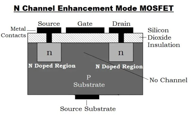
p-channel: The construction of a p-channel enhancement-type MOSFET is exactly the reverse of that of n-channel. That is, there is now an n-type substrate and p-doped regions under the drain and source connections.
